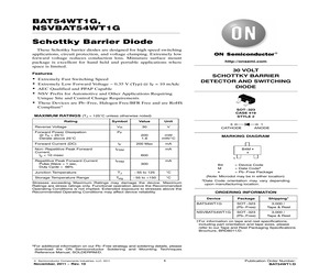
NSVBAT54WT1G Schottky Barrier Diode These Schottky barrier diodes are designed for high speed switching applications, circuit protection, and voltage clamping. Extremely low forward voltage reduces conduction loss. Miniature surface mount package is excellent for hand held and portable applications where space is limited. Features Extremely Fast Switching Speed Extremely Low Forward Voltage - 0.35 V (Typ) @ IF = 10 mAdc AEC Qualified and PPAP Capable NSV Prefix for Automotive and Other Applications Requiring Unique Site and Control Change Requirements These Devices are Pb-Free, Halogen Free/BFR Free and are RoHS Compliant* http://onsemi.com 30 VOLT SCHOTTKY BARRIER DETECTOR AND SWITCHING DIODE SOT-323 CASE 419 STYLE 2 MAXIMUM RATINGS (TJ = 125C unless otherwise noted) Symbol Value Unit Reverse Voltage VR 30 V Forward Power Dissipation @ TA = 25C Derate above 25C PF 200 1.6 mW mW/C Forward Current (DC) IF 200 Max mA Rating Non-Repetitive Peak Forward Current, tp < 10 msec IFSM Repetitive Peak Forw
 4 Pages, 126 KB, Original
M G = Device Code = Date Code* = Pb-Free Package (Note: Microdot may be in either location) *Date Code orientation may vary depending upon manufacturing location. ORDERING INFORMATION Device Package Shipping BAT54WT1G SOT-323 (Pb-Free) 3,000 / Tape & Reel NSVBAT54WT1G SOT-323 (Pb-Free) 3,000 / Tape & Reel For information on tape and reel specifications, including part orientation and tape sizes, please refer to our Tape and Reel Packaging Specifications Brochure, BRD8011/D. *For additional information on our Pb-Free strategy and soldering details, please download the ON Semiconductor Soldering and Mounting Techniques Reference Manual, SOLDERRM/D. (c) Semiconductor Components Industries, LLC, 2014 October, 2018 - Rev. 12 1 Publication Order Number: BAT54WT1/D BAT54W ELECTRICAL CHARACTERISTICS (TA = 25C unless otherwise noted) Symbol Characteristic Reverse Breakdown Voltage (IR = 10 mA) V(BR)R Total Capacitance (VR = 1.0 V, f = 1.0 MHz) CT Reverse Leakage (VR = 25 V) IR Forward Voltage (IF = 0.1 mA
 5 Pages, 101 KB, Original
M G = Device Code = Date Code* = Pb-Free Package (Note: Microdot may be in either location) *Date Code orientation may vary depending upon manufacturing location. ORDERING INFORMATION Device Package Shipping BAT54WT1G SOT-323 (Pb-Free) 3,000 / Tape & Reel NSVBAT54WT1G SOT-323 (Pb-Free) 3,000 / Tape & Reel For information on tape and reel specifications, including part orientation and tape sizes, please refer to our Tape and Reel Packaging Specifications Brochure, BRD8011/D. *For additional information on our Pb-Free strategy and soldering details, please download the ON Semiconductor Soldering and Mounting Techniques Reference Manual, SOLDERRM/D. (c) Semiconductor Components Industries, LLC, 2014 October, 2018 - Rev. 12 1 Publication Order Number: BAT54WT1/D BAT54W ELECTRICAL CHARACTERISTICS (TA = 25C unless otherwise noted) Symbol Characteristic Reverse Breakdown Voltage (IR = 10 mA) V(BR)R Total Capacitance (VR = 1.0 V, f = 1.0 MHz) CT Reverse Leakage (VR = 25 V) IR Forward Voltage (IF = 0.1 mA
 4 Pages, 91 KB, Original
M G = Device Code = Date Code* = Pb-Free Package (Note: Microdot may be in either location) *Date Code orientation may vary depending upon manufacturing location. ORDERING INFORMATION Device Package Shipping BAT54WT1G SOT-323 (Pb-Free) 3,000 / Tape & Reel NSVBAT54WT1G SOT-323 (Pb-Free) 3,000 / Tape & Reel For information on tape and reel specifications, including part orientation and tape sizes, please refer to our Tape and Reel Packaging Specifications Brochure, BRD8011/D. *For additional information on our Pb-Free strategy and soldering details, please download the ON Semiconductor Soldering and Mounting Techniques Reference Manual, SOLDERRM/D. (c) Semiconductor Components Industries, LLC, 2014 October, 2018 - Rev. 12 1 Publication Order Number: BAT54WT1/D BAT54W ELECTRICAL CHARACTERISTICS (TA = 25C unless otherwise noted) Symbol Characteristic Reverse Breakdown Voltage (IR = 10 mA) V(BR)R Total Capacitance (VR = 1.0 V, f = 1.0 MHz) CT Reverse Leakage (VR = 25 V) IR Forward Voltage (IF = 0.1 mA
 5 Pages, 165 KB, Original


