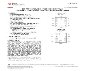
........................................................................................................................................... www.ti.com ORDERING INFORMATION TA -40C to 85C (1) (2) PACKAGE QFN - RSE (1) (2) ORDERABLE PART NUMBER Reel of 3000 TS3USB221ARSER TOP-SIDE MARKING LHR Package drawings, thermal data, and symbolization are available at www.ti.com/packaging. For the most current package and ordering information, see the Package Option Addendum at the end of this document, or see the TI website at www.ti.com. PIN DESCRIPTION NAME DESCRIPTION OE Bus-switch enable S Select input D Bus A nD Bus B TRUTH TABLE S OE FUNCTION X H Disconnect L L D = 1D H L D = 2D BLOCK DIAGRAM D+ 1D+ D- 1D- 2D+ 2D- S OE SIMPLIFIED SCHEMATIC, EACH FET SWITCH (SW) A B VCC Charge Pump EN (see Note A) A. 2 EN is the internal enable signal applied to the switch. Submit Documentation Feedback Copyright (c) 2008, Texas Instruments Incorporated Product Folder Link(s): TS3USB221A TS3USB221A www.ti.com .........
 17 Pages, 1129 KB, Original
........................................................................................................................................... www.ti.com ORDERING INFORMATION TA -40C to 85C (1) (2) PACKAGE QFN - RSE (1) (2) ORDERABLE PART NUMBER Reel of 3000 TS3USB221ARSER TOP-SIDE MARKING LHR Package drawings, thermal data, and symbolization are available at www.ti.com/packaging. For the most current package and ordering information, see the Package Option Addendum at the end of this document, or see the TI website at www.ti.com. PIN DESCRIPTION NAME DESCRIPTION OE Bus-switch enable S Select input D Bus A nD Bus B TRUTH TABLE S OE FUNCTION X H Disconnect L L D = 1D H L D = 2D BLOCK DIAGRAM D+ 1D+ D- 1D- 2D+ 2D- S OE SIMPLIFIED SCHEMATIC, EACH FET SWITCH (SW) A B VCC Charge Pump EN (see Note A) A. 2 EN is the internal enable signal applied to the switch. Submit Documentation Feedback Copyright (c) 2008, Texas Instruments Incorporated Product Folder Link(s): TS3USB221A TS3USB221A www.ti.com .........
 18 Pages, 1135 KB, Original
........................................................................................................................................... www.ti.com ORDERING INFORMATION TA -40C to 85C (1) (2) PACKAGE QFN - RSE (1) (2) ORDERABLE PART NUMBER Reel of 3000 TS3USB221ARSER TOP-SIDE MARKING LHR Package drawings, thermal data, and symbolization are available at www.ti.com/packaging. For the most current package and ordering information, see the Package Option Addendum at the end of this document, or see the TI website at www.ti.com. PIN DESCRIPTION NAME DESCRIPTION OE Bus-switch enable S Select input D Bus A nD Bus B TRUTH TABLE S OE FUNCTION X H Disconnect L L D = 1D H L D = 2D BLOCK DIAGRAM D+ 1D+ D- 1D- 2D+ 2D- S OE SIMPLIFIED SCHEMATIC, EACH FET SWITCH (SW) A B VCC Charge Pump EN (see Note A) A. 2 EN is the internal enable signal applied to the switch. Submit Documentation Feedback Copyright (c) 2008, Texas Instruments Incorporated Product Folder Link(s): TS3USB221A TS3USB221A www.ti.com .........
 17 Pages, 848 KB, Original
........................................................................................................................................... www.ti.com ORDERING INFORMATION TA -40C to 85C (1) (2) PACKAGE QFN - RSE (1) (2) ORDERABLE PART NUMBER Reel of 3000 TS3USB221ARSER TOP-SIDE MARKING LHR Package drawings, thermal data, and symbolization are available at www.ti.com/packaging. For the most current package and ordering information, see the Package Option Addendum at the end of this document, or see the TI website at www.ti.com. PIN DESCRIPTION NAME DESCRIPTION OE Bus-switch enable S Select input D Bus A nD Bus B TRUTH TABLE S OE FUNCTION X H Disconnect L L D = 1D H L D = 2D BLOCK DIAGRAM D+ 1D+ D- 1D- 2D+ 2D- S OE SIMPLIFIED SCHEMATIC, EACH FET SWITCH (SW) A B VCC Charge Pump EN (see Note A) A. 2 EN is the internal enable signal applied to the switch. Submit Documentation Feedback Copyright (c) 2008, Texas Instruments Incorporated Product Folder Link(s): TS3USB221A TS3USB221A www.ti.com .........
 18 Pages, 1135 KB, Original
........................................................................................................................................... www.ti.com ORDERING INFORMATION TA -40C to 85C (1) (2) PACKAGE QFN - RSE (1) (2) ORDERABLE PART NUMBER Reel of 3000 TS3USB221ARSER TOP-SIDE MARKING LHR Package drawings, thermal data, and symbolization are available at www.ti.com/packaging. For the most current package and ordering information, see the Package Option Addendum at the end of this document, or see the TI website at www.ti.com. PIN DESCRIPTION NAME DESCRIPTION OE Bus-switch enable S Select input D Bus A nD Bus B TRUTH TABLE S OE FUNCTION X H Disconnect L L D = 1D H L D = 2D BLOCK DIAGRAM D+ 1D+ D- 1D- 2D+ 2D- S OE SIMPLIFIED SCHEMATIC, EACH FET SWITCH (SW) A B VCC Charge Pump EN (see Note A) A. 2 EN is the internal enable signal applied to the switch. Submit Documentation Feedback Copyright (c) 2008, Texas Instruments Incorporated Product Folder Link(s): TS3USB221A TS3USB221A www.ti.com .........
 17 Pages, 752 KB, Original
........................................................................................................................................... www.ti.com ORDERING INFORMATION TA -40C to 85C (1) (2) PACKAGE QFN - RSE (1) (2) ORDERABLE PART NUMBER Reel of 3000 TS3USB221ARSER TOP-SIDE MARKING LHR Package drawings, thermal data, and symbolization are available at www.ti.com/packaging. For the most current package and ordering information, see the Package Option Addendum at the end of this document, or see the TI website at www.ti.com. PIN DESCRIPTION NAME DESCRIPTION OE Bus-switch enable S Select input D Bus A nD Bus B TRUTH TABLE S OE FUNCTION X H Disconnect L L D = 1D H L D = 2D BLOCK DIAGRAM D+ 1D+ D- 1D- 2D+ 2D- S OE SIMPLIFIED SCHEMATIC, EACH FET SWITCH (SW) A B VCC Charge Pump EN (see Note A) A. 2 EN is the internal enable signal applied to the switch. Submit Documentation Feedback Copyright (c) 2008, Texas Instruments Incorporated Product Folder Link(s): TS3USB221A TS3USB221A www.ti.com .........
 17 Pages, 847 KB, Original
........................................................................................................................................... www.ti.com ORDERING INFORMATION TA -40C to 85C (1) (2) PACKAGE QFN - RSE (1) (2) ORDERABLE PART NUMBER Reel of 3000 TS3USB221ARSER TOP-SIDE MARKING LHR Package drawings, thermal data, and symbolization are available at www.ti.com/packaging. For the most current package and ordering information, see the Package Option Addendum at the end of this document, or see the TI website at www.ti.com. PIN DESCRIPTION NAME DESCRIPTION OE Bus-switch enable S Select input D Bus A nD Bus B TRUTH TABLE S OE FUNCTION X H Disconnect L L D = 1D H L D = 2D BLOCK DIAGRAM D+ 1D+ D- 1D- 2D+ 2D- S OE SIMPLIFIED SCHEMATIC, EACH FET SWITCH (SW) A B VCC Charge Pump EN (see Note A) A. 2 EN is the internal enable signal applied to the switch. Submit Documentation Feedback Copyright (c) 2008, Texas Instruments Incorporated Product Folder Link(s): TS3USB221A TS3USB221A www.ti.com .........
 16 Pages, 725 KB, Original
........................................................................................................................................... www.ti.com ORDERING INFORMATION TA -40C to 85C (1) (2) PACKAGE QFN - RSE (1) (2) ORDERABLE PART NUMBER Reel of 3000 TS3USB221ARSER TOP-SIDE MARKING LHR Package drawings, thermal data, and symbolization are available at www.ti.com/packaging. For the most current package and ordering information, see the Package Option Addendum at the end of this document, or see the TI website at www.ti.com. PIN DESCRIPTION NAME DESCRIPTION OE Bus-switch enable S Select input D Bus A nD Bus B TRUTH TABLE S OE FUNCTION X H Disconnect L L D = 1D H L D = 2D BLOCK DIAGRAM D+ 1D+ D- 1D- 2D+ 2D- S OE SIMPLIFIED SCHEMATIC, EACH FET SWITCH (SW) A B VCC Charge Pump EN (see Note A) A. 2 EN is the internal enable signal applied to the switch. Submit Documentation Feedback Copyright (c) 2008, Texas Instruments Incorporated Product Folder Link(s): TS3USB221A TS3USB221A www.ti.com .........
 17 Pages, 876 KB, Original
........................................................................................................................................... www.ti.com ORDERING INFORMATION TA -40C to 85C (1) (2) PACKAGE QFN - RSE (1) (2) ORDERABLE PART NUMBER Reel of 3000 TS3USB221ARSER TOP-SIDE MARKING LHR Package drawings, thermal data, and symbolization are available at www.ti.com/packaging. For the most current package and ordering information, see the Package Option Addendum at the end of this document, or see the TI website at www.ti.com. PIN DESCRIPTION NAME DESCRIPTION OE Bus-switch enable S Select input D Bus A nD Bus B TRUTH TABLE S OE FUNCTION X H Disconnect L L D = 1D H L D = 2D BLOCK DIAGRAM D+ 1D+ D- 1D- 2D+ 2D- S OE SIMPLIFIED SCHEMATIC, EACH FET SWITCH (SW) A B VCC Charge Pump EN (see Note A) A. 2 EN is the internal enable signal applied to the switch. Submit Documentation Feedback Copyright (c) 2008, Texas Instruments Incorporated Product Folder Link(s): TS3USB221A TS3USB221A www.ti.com .........
 17 Pages, 839 KB, Original
........................................................................................................................................... www.ti.com ORDERING INFORMATION TA -40C to 85C (1) (2) PACKAGE QFN - RSE (1) (2) ORDERABLE PART NUMBER Reel of 3000 TS3USB221ARSER TOP-SIDE MARKING LHR Package drawings, thermal data, and symbolization are available at www.ti.com/packaging. For the most current package and ordering information, see the Package Option Addendum at the end of this document, or see the TI website at www.ti.com. PIN DESCRIPTION NAME DESCRIPTION OE Bus-switch enable S Select input D Bus A nD Bus B TRUTH TABLE S OE FUNCTION X H Disconnect L L D = 1D H L D = 2D BLOCK DIAGRAM D+ 1D+ D- 1D- 2D+ 2D- S OE SIMPLIFIED SCHEMATIC, EACH FET SWITCH (SW) A B VCC Charge Pump EN (see Note A) A. 2 EN is the internal enable signal applied to the switch. Submit Documentation Feedback Copyright (c) 2008, Texas Instruments Incorporated Product Folder Link(s): TS3USB221A TS3USB221A www.ti.com .........
 15 Pages, 597 KB, Original
........................................................................................................................................... www.ti.com ORDERING INFORMATION TA -40C to 85C (1) (2) PACKAGE QFN - RSE (1) (2) ORDERABLE PART NUMBER Reel of 3000 TS3USB221ARSER TOP-SIDE MARKING LHR Package drawings, thermal data, and symbolization are available at www.ti.com/packaging. For the most current package and ordering information, see the Package Option Addendum at the end of this document, or see the TI website at www.ti.com. PIN DESCRIPTION NAME DESCRIPTION OE Bus-switch enable S Select input D Bus A nD Bus B TRUTH TABLE S OE FUNCTION X H Disconnect L L D = 1D H L D = 2D BLOCK DIAGRAM D+ 1D+ D- 1D- 2D+ 2D- S OE SIMPLIFIED SCHEMATIC, EACH FET SWITCH (SW) A B VCC Charge Pump EN (see Note A) A. 2 EN is the internal enable signal applied to the switch. Submit Documentation Feedback Copyright (c) 2008, Texas Instruments Incorporated Product Folder Link(s): TS3USB221A TS3USB221A www.ti.com .........
 15 Pages, 598 KB, Original
ode TPS54331D 03-03825-33 Processor Supervisory Circuits TPS3825-33DBVT U1033 03-00717-01 TinyLogic UHS Dual Buffer with Schmitt Trigger NC7WZ17 U1032, U1034 03-00221-02 High-Speed USB 2.0 (480 Mbps) 1:2 Multiplexer/Demultiplexer Switch With Single Enable TS3USB221ARSER U1029 03-32460-02 PIC32 MCUs (Microcontrollers) 512KB PIC32MX460F512L-80I/PT U1027 33-20012-01 33-20336-01 SCHOTTKY DIODE SMD SCHOTTKY DIODE SMD SS12 SMA SS36, SCHOTTKY,60V D1002 D1004 U1016 U1035 () HS40-C390DD_B17VM1.4 VM1.4 for MP 2012-03-19 C390DD BOM 33-40352-01 Switch Diode 1SS352(TPH3,F),1SS355TE-17 33-13609-10 33-14709-10 Zener Diode Zener Diode 3.6V, 0.5W LL34 4V7,1/2W, LL34 31-00114-01 Digital transistors (built-in resistors) D6201, D6202, D6203, D6204, D6205, D6206, D6210, D6212 D1003 D1000,D1001, D1005, D1006 Transistor DTA114EKA Q1013 31-00114-05 Digital Transistor(Built in Resistor) DTC114EKA Q1003, Q1004, Q1007, Q1008, Q1011, Q1014,Q1000, Q1012 31-02301-01 P-Channel Enhancement Mode MOSFET APM2301 Q1001, Q1002, Q100
 88 Pages, 5602 KB, Original
 Optional Serial EEPROM Interface 4-Port USB Hub Power Controller TPS2075DB 7-Port USB Hub W/Optional Serial TUSB2077APT EEPROM Interface General-Purpose USB Device Controller TUSB3210PM USB-to-Serial Port Controller W/ TUSB3410VF 3 IN and 3 OUT endpoints TS3USB221ARSER High-Speed USB 2.0 (480-Mbps) 1:2 MUX/ DEMUX Switch with Single Enable TS3USB221EDRCR High-Speed USB 2.0 (480-Mbps) 1:2 MUX/ DEMUX Switch with Single Enable TS3USB221ERSER High-Speed USB 2.0 (480-Mbps) 1:2 MUX/ DEMUX Switch with Single Enable TS3USB31ERSER High-Speed USB 2.0 (480-Mbps) 1-Port Switch With Single Enable TS5USBA224RSWR High-Speed USB 2.0 (480Mbps) & Audio Switches with Negative Signal Capability Price Each 1-24 1.93 1.65 Pkg. 16-QFN Stock No. 78M6644 16-QFN 27M1136 1.71 1.23 16-TSSOP 31M0466 1.93 1.35 32-LQFP 77C1805 4.06 3.01 32-QFN 14N8499 4.20 2.85 24-SSOP 48-LQFP 77C0038 77C1807 9.63 7.09 6.58 5.79 64-LQFP 32-LQFP 35K1366 36K2070 7.88 5.58 6.75 5.94 10-QFN 46P4286 2.10 1.80 10-SON 91R2096 2.10 1.80 10-UQFN 91R209
 375 Pages, 58008 KB, Original


